We are the test lab of the future, built on a foundation of innovation, precision, and agility. Established with a steadfast commitment to advancing semiconductor testing, we specialize in cutting-edge electrical testing and comprehensive reliability testing. Our mission is to validate new products, processes, and packages with unparalleled accuracy, ensuring they meet the highest standards of performance and reliability.
As a futuristic testing lab, we are equipped to handle the most demanding challenges in semiconductor validation, from wafer-level and die-level to package-level testing. Our expertise lies in tailoring custom testing solutions to your specific needs, enabling rapid market deployment across diverse industries. With a 24/7 round-the-clock engagement model and concurrent engineering capabilities, we ensure seamless collaboration and faster time-to-market for your products.
We provide leading-edge electrical testing and reliability testing services, accelerating your time to market. Whether you’re developing new products, refining existing technologies, or working on R&D projects, we deliver rapid and precise assessments to ensure your success.
Our services are designed to support a wide range of semiconductor applications, including ASICs, ASSPs, and complex processors tailored for industries such as automotive, commercial and military aerospace, communications, radar systems, instrumentation, connectivity, artificial intelligence, and digital signal processing.
We are at the forefront of the semiconductor industry, specializing in the testing of smart AI chips, next-generation processors, and high-performance computing (HPC) chips. From neural network accelerators to legacy-free test programs, our advanced testing capabilities ensure these cutting-edge technologies meet the highest standards of performance, reliability, and power efficiency.
With remote connectivity for customers and tester availability across global locations, including our Israel development center (iTest IL), we provide integrated support throughout the development, debugging, and reliability benchmarking processes.
We specialize in futuristic package evaluation, ultra-high-density semiconductor testing, and advanced electrical testing, including System on Chip (SoC) and System in Package (SiP) designs. Our team excels in developing custom testing solutions that address the unique challenges of advanced technologies, ensuring your products perform reliably and meet stringent electrical performance standards under real-world conditions.
for production and characterization.
to validate design performance.
for comprehensive validation.
to reduce predicted time and accelerate development cycles.
We support the latest advancements in semiconductor design and packaging.
Custom testing and reliability plans designed for your specific technology and application.
Accelerated testing and validation processes to meet tight deadlines.
A team of skilled engineers dedicated to solving your most complex challenges.
A relentless focus on enabling your success through collaboration and agility.
With facilities like our Israel development center, we offer 24/7 engagement to serve customers worldwide.
We are committed to helping you achieve market success by delivering reliable, high-performance semiconductor solutions. Whether you’re developing next-generation technologies or refining existing products, we are your trusted partner in electrical and reliability testing.
Let us help you navigate the complexities of semiconductor validation and bring your innovations to market faster, with confidence.
We work closely with you to understand your testing needs and challenges.
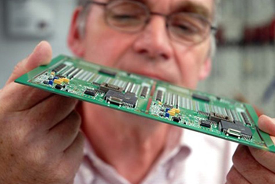
We are the discerning I, the test lab of the future, established with a staunch purpose to build upon the cutting edge, leading edge ATE test development, load board development capability and provide the secondary extension of electrical test which is to validate a new product, a new process, or a new package.
We are a futuristic reliability lab set up to offer wafer process and foundry qualification while qualifying package technologies in their worst-case use environment. Our unwavering expertise is to tailor your reliability plans and enable you to develop standard qualification guidelines expediting the quick market deployment in various business sectors. We specialize in ASICs, AASPs, Complex processors suited for the Automotive, Commercial and Military space, communication, radars, instrumentations, connectivity, artificial intelligence, digital signal processing and others. We are razor focused to get you to the market with the shortest, swiftest possible technology packaging validation, and assist you in getting acknowledged into the marketplace as a qualified product.
Our Qualification Plans are designed to target reliability efforts tailored to a specific technology and a customer in a specific application sector. To accentuate , what we offer is custom reliability plans, custom solutions, custom application conditions, custom and realistic ways of being able to do reliability testing with optimal sample sizes. We build upon the wafer data, the process data, the in-process data, the packaging data, the design data and design custom reliability quality plans to ensure your success in the shortest span of time.
We work with the customer and do quick validation of your design, quick ESD, quick latch up, quick thermal function tests followed by test for reliability acceptance. In addition to this, we will do a technology evaluation, limited qual, followed by a personalized plan to defining qual plans, sample sizes, reliability targets and the reliability predictions with failure rate calculations.
Our forte is to support cutting edge technology, ultra-high integration, ultra-high density, sub 28 nanometer technology where complexity and integration of the design, that is more like a System on Chip (SoC) or a System in Package ( Sip) requires very unique and creative reliability methodologies to be able to qualify and validate their technology.
Futuristic Package Evaluation, package in terms of size, validation, Thermal Moir ’e imaging, warpage analysis, structural analysis of a package, coefficients of TC thermal coefficients matching, materials matching, followed by reliability standards and benchmarks are our prized niche.
Along with this, we are a lab that is focused on understanding the realities of no human contact electronic lab. A lab with key focus on electronic control of power supplies and media, voltage tolerances, temperature controls, thermal junction measurements, junction regulation, ambient regulation. Our reliability instrumentation with all its tenacity, nurtures progression while a talented engineering group will strive effectively to provide unique custom solutions for each futuristic reliability evaluation.